Elements of computing systems
Introduction
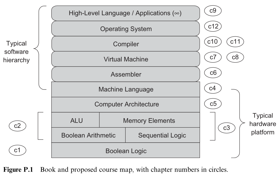
These are the notes which I took while studying computer architecture from the textbook “The Elements of Computing Systems by Noam Nisan & Shimon Schocken “. They’re very terse and have very opinionated content from the textbook so they should only be used in tandem with it for revision purposes.
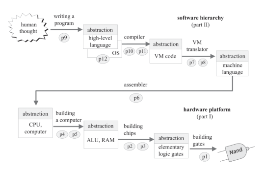
 The text program is parsed, its semantics are uncovered, it’s represented in some low-level language that the computer can understand. This process is called compilation. Its result is another text file, containing machine-level code.
To make this abstract machine code concrete, it has to be realized by some hardware architecture which is implemented by a chipset - registers, memory, ALU, etc. These devices are made of logic gates which consist of switching devices that are implemented by transistors.
Church-Turing conjecture: At their core, all computers are essentially equivalent.
Boolean Logic
Any boolean function can be realised by just the nand gate. Let that sink in. A gate is a physical device that implements a simple boolean function. They are implemented as transistors etched in silicon, packaged as chips. The boolean function chip is designed and tested by using a Hardware Description Language (HDL). This simulated realisation is then tested for corectness and other parameters such as speed of computation, energy consumption and cost are quantified. To illustrate the same proces, HDL implementation of a XOR function is shown below.
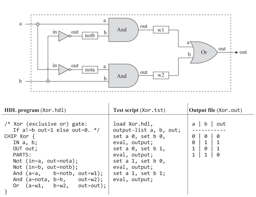
Using built-in libarary chips is similar to writing a regular program except the PARTS section is replaced with BUILTIN Xor. Some things to note are that internal pins are created automatically when they appear in an HDL program and that pins may have an unlimited fan-out. In HDL programs, the existence of forks is inferred from the code.
Chips are specified using the API style, for nand gate:
Chip name: Nand
Input: a,b
Output: out
Function: if ((a==1) and (b==1)) then out = 0, else out = 1
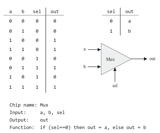
Multiplexer: Has two input(data) bits a,b and one selection bit sel which decides which input bit would be the output.
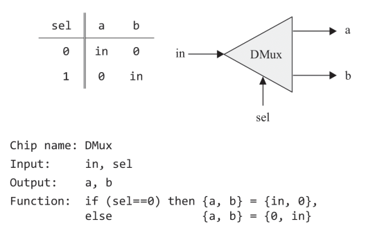
Demultiplexer: Takes in a single input and routes it to one of the possible outputs depeding on the selector bit.
HDL programs treat multi-bit values like single-bit values but they are indexed(from right to left, rightmost being 0\(^{th}\) bit) to access individual bits. For example, a m-way n-bit mux would select one of its m n-bit inputs and output it to its n-bit output, where there would be \(k=log_{2}m\) selection bits. A 4-way 16-bit mux API would look like:
Chip name: Mux4Way16
Input: a[16],b[16],c[16],d[16],sel[2]
Output: out[16]
Function: if(sel==00,01,10, or 11) then out = a,b,c, or d
Comment: The assignment is a 16-bit operation. For example, "out = a" means "for i = 0..15 out[i] = a[i]"
Boolean Arithmetic
Word size is a term used for specifying the number of bits that computers use for representing a basic chunk of values. For example, integer values are stored in 8-, 16-, 32- or 64-bit registers. Fixed word size implies the existence of a limit on number of values that the registers can represent. In general, using n bits, one can represent values from 0 to 2\(^{n}\) - 1.
Addition
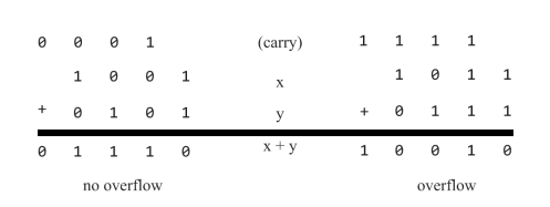
If the most significant bitwise addition generates a carry of 1, overflow occurs, if that is ignored, one achieves n correct bits for adding two n-bit numbers.
Signed Numbers
The coding scheme was chosen so that hardware implementation of arithmetic operations would be as simple as possible, its result being two’s complement binary code that represents negative x as binary code that represents 2\(^{n}\) - x. For example, in a 4-bit binary system -5 would be represented as binary of (16-5) or 1011. This leads us to the following properties:
- For an n-bit system, 2\(^{n}\) signed numbers are generated, from -(2\(^{n-1}\)) to 2\(^{n-1}\) - 1.
- Code for positive numbers begins with 0 while for negatives with 1.
- To get code of -x from x, flip all bits of x and add 1.
Adders
Half adder: Adds two numbers/bits and outputs in for of sum and carry which are LSB and MSB of the addition of the input bits.
Full adder: Adds three bits and outputs the result in form of sum and carry bits.
Adder: Adds two n-bit numbers and outputs as out, which is also n-bit. Here the overflow bit is ignored.
Incrementer: Adds 1 to a given number, enables fetching next instruction from memory after executing the current.
Note that this adder implementation is inefficient because of delays incurred by propogation of carry bits which can be acclerated by carry lookahead heuristics.
ALU
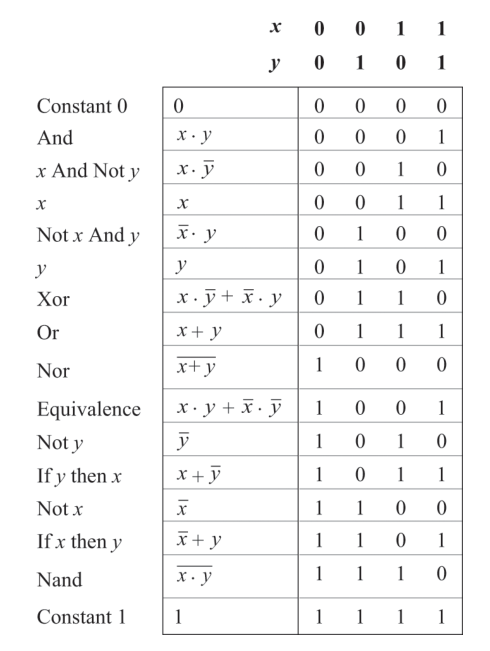
Designed to compute a set of arithmetic and logic operations, exactly which ones is a design decision derived from cost-effectiveness considerations. Shown below is the Hack ALU which computes 18 functions which are controlled by six 1-bit control bits. In addition to those there are zr and ng bits which flag whether the output is zero or negative. Note that the output overflow bit is ignored.
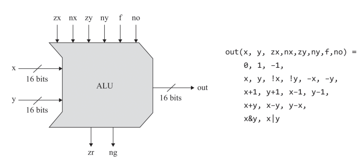
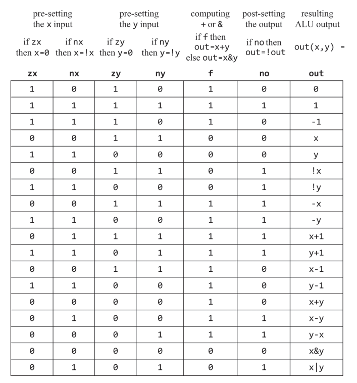
To illustrate the ALU logic, if one wishes to compute x-1 for x=27, then control bits would be 001110. These six directives are to be performed in order: first, we either set the x and y inputs to 0, or not; next, we either negate the resulting values, or not; then we compute either + or & on the preprocessed values; and finally, we either negate the resulting value, or not. The first two 00 show that we neither zero nor negate x, then 11 shows that we zero y and then negate it, leading to 16-bit value 1111111111111111 which is -1 in two’s complement. The next control bit 1 dictates addition operation and the last 0 bit shows that output shouldn’t be negated hence we get the desired function x-1.
Memory
All the chips considered so far are time independent, they’re called combinational chips. Now sequential chips are introduced whose output depends not only on current time inputs but past inputs and outputs too. The notion of time is introduced by a clock that generates a cycle of binary singals that are called a tick and a tock.
By viewing the time in the form of cycles instead of a continuous progression, the changes in the system are made atomic i.e. they’ll only be reflected during cycle transitions and within a cycle, no change would be shown. This discrete view helps in neutralizing randomness associated with time delays and can be used for synchronizing the operations of different chips. For that, the cycle should be long enough to contain the possible time delay but short enough so that the resulting system’s fast because the changes would only be shown during transitions.
Also, to ensure output validity duration of the clock cycle has to be slightly longer than the time it takes a bit to travel the longest distance from one chip to another, plus the time it takes to complete the most time-consuming within-chip calculation.
Flip Flops
A Data flip-flip (DFF) is a memory chip which has a single-bit data input and output and an addition clock input(marked by small triangle on gate icon) that feeds from master clock’s signal. It models the behavior out(t)=in(t-1) that is, in every subsequent time unit, DFF outputs input from previous time unit. At all other times, DFFs are latched, meaning that changes in their inputs have no immediate effect on the output.
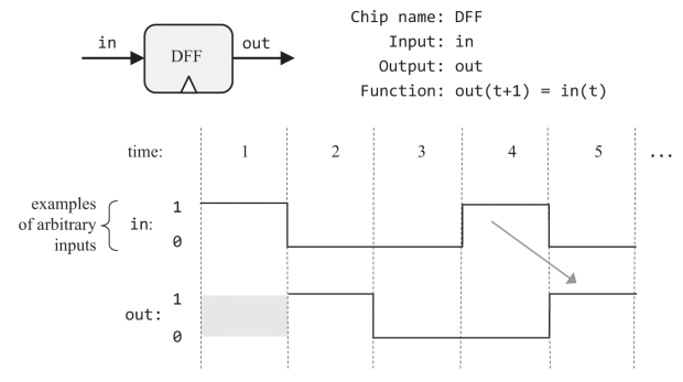
Note that the concept of feedback loops doesn’t make sense in combinational chips, but there is no difficulty in feeding outputs back into inputs if they’re passed through a DFF gate so that the output at time t does not depend on itself but rather on the output at time t-1.
FFs are generally constructed from nand gates connected in feedback loops. The standard construction begins by building a non-clocked flip-flop which is bi-stable, that is, can be set to be in one of two states (storing 0, and storing 1). Then a clocked flip-flop is obtained by cascading two such non-clocked flip-flops, the first being set when the clock ticks and the second when the clock tocks.
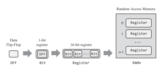
Registers
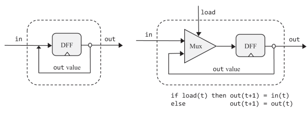
A register is a DFF with a load input. It stores and outputs its current value until load instructs it to update to a new value.
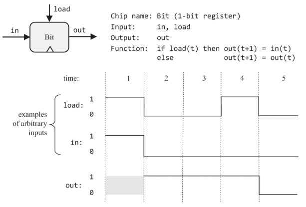
A 16-bit register behaves the same as a bit chip, just that it deals with 16-bit values. A register fulfils the classical function of a memory device, remember and emit the last written value, until its set to another.
RAM
A RAM chip consists of n 16-bit register chips which can be selected and manipulated separately. By specifying a particular address (0 to n-1), a particular register can be selected for read/write operations. Note that the access time of any randomly selected register is instantaneous.
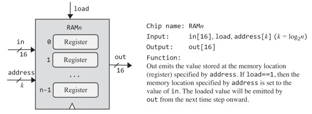
RAM implementations can be modular, for example one could implement RAM64 i.e. having 64 registers by using eight RAM8 chips, to select a particular register one uses a 6-bit address xxxyyy where xxx bits can be used to select one of the RAM8 chips and yyy bits can be used to select the register within the RAM8 chip.
Counter
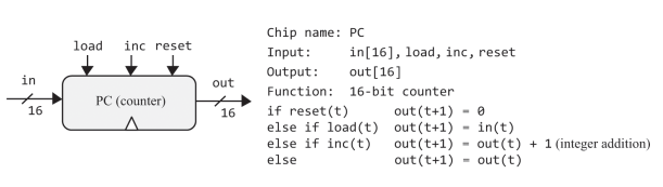
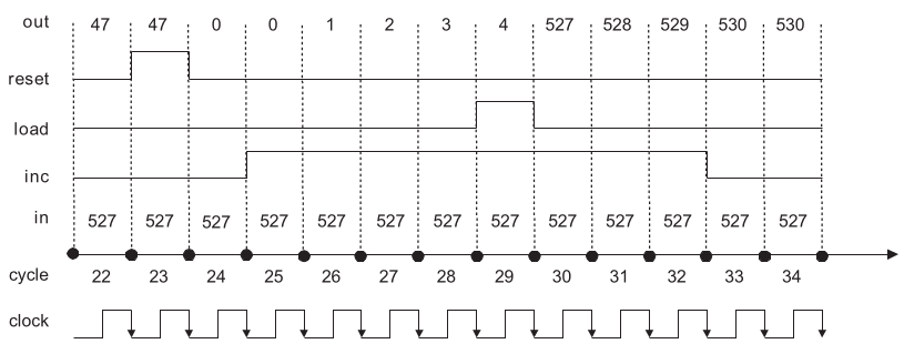
A chip that’s implementation of an incrementer used to keep track of program instructions (PC: Program Counter). It has three functional inputs alongwith in, namely inc, which increases counter state every cycle(PC++) and reset which sets it to 0 and load sets its value to whatever values is fed by in.
Machine Language
“Form follows function.”
A machine language can be viewed as an agreed-upon formalism designed to manipulate a memory using a processor and a set of registers. Unlike high-level languages, whose design goals are cross-platform compatibility and power of expression, machine languages are designed to effect direct execution in a specific hardware platform and its control. For this project, Hack machine language is used.
Machine language programs can be written in either binary or symbolic instructions. Programs writtern in symbolic(assembly) languages are translated into executable binary code by a translator program called assembler.
Hardware
Memory: Functionally speaking, a memory is a continuous sequence of cells, also referred to as locations or memory registers, each having a unique address.
Processor: A device capable of performing a fixed set of primitve operations which include arithmetic, logical, memory access and control/branching operations.
Registers: Inside the processor’s chip, they serve as high-speed local memory, allowing it to manipulate data and instructions without having to be dependent on slow memory chips. They’re categorized into data and address registers.
Instructions
Arithmetic and logical operations: Assuming that the processor has a set of registers denoted R0, R1, R2,.... Basic operations like addition, subtraction, and(bitwise), or, not.
load R1,true
load R2,false
and R1,R2,R2 (R1 ← R1 And R2)
Memory access: Using address register A, let us set memory location 17 to value 1.
load A,17
load M,1
Here by convention, M stands for memory register selected by A.
Flow control: For facilitating branching actions, labelled goto statements exist.
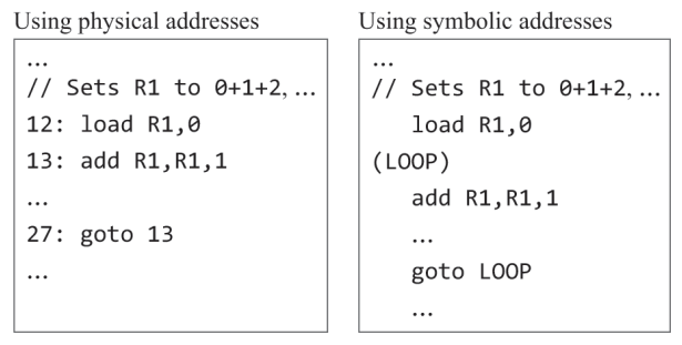
Symbols: Make it easier to not rely on rigid physical addresses which makes the code relocatable.
Hack
Memory: Hack uses two distinct memory units, data and instruction memory. Both memories are 16-bit wide, and each has a 15-bit address space, hence maximum addressable size of each memory unit is 2\(^{15}\) or 32K 16-bit words.
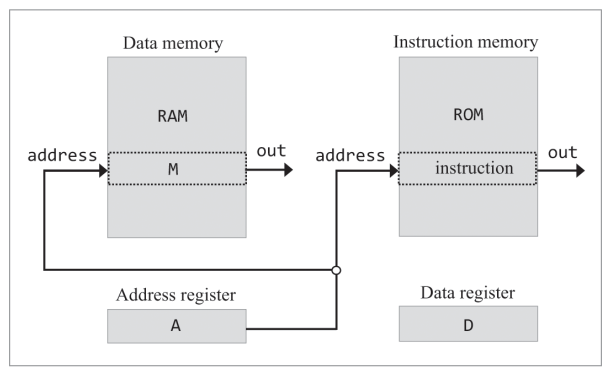
Data memory’s address input always contains some value so there’s always one selected register called M. Instruction memory’s address input also always contains some value that is, there’s always one selected instruction memory register whose value is referred to as current instruction.
Registers: Hack Instructions work on three 16-bit registers, data (D: stores value), address (A: both address and data) and selected data memory register M. To store a constant in A register, instruction is @17, to set D register to a value, two instructions are needed: @17 then D=A.
Addressing: The @xxx instruction does two things, first it makes the RAM register whose address is xxx the selected memory register(M) and then it makes the value of the ROM register whose address is xxx the selected instruction. For example, to set value of RAM[100] to 17, instructions are @17, D=A, @100, M=D. Initially A acts as a data register then as an address register. To set value of RAM[100] to value of RAM[200], do @200, D=M, @100, M-D.
Branching: